Describe The Working Of A Full Adder Circuit
Question
Task:
Part 1:
Using the CMOS integrated circuits, design a combinational full adder circuit system with the help of a digital arithmetic system.
Considering every logic level, check the working of the circuit. With the help of data sheets, compare the specifications of your circuit with AND, OR and Exclusive OR gates. Validate your assessment using truth tables.
Evaluate the differences in the working of a Sequential and combinational logic devices in a Full Adder Circuit.
Part 2:
Assess and recommend changes to a digital system's circuit process with respect to the data acquisition approach and the interface used. Bearing in mind the alarm system that you have used for measuring, monitoring and performance tuning of the circuit.
Understand and analyse how the system works in terms of collecting the information and communicating the findings within its service, indicating possible improvements.
Understand and propose enhancements to the human interaction with the Full Adder Circuit.
Answer
Digital Logic Circuit:
For the functioning of digital logic circuits, distinct voltage scales should be used. Digital circuits utilise abstract circuit components. Gates are called the abstract components of the circuit The gate's output is the input variable. Digital circuits resolve noise interference and signal attenuation in case of analogue circuits. Two types of digital circuits exist:
- Digital Logic Circuits
- Combination Logic Circuits
Combinational Logic Circuits
A combination logic circuit's output is a variable of the existing input. Therefore, in a combinational full adder circuit a state can not be retained. The calculation actions on stored information are carried out by combinational logic circuits. Types of combinational logic circuits such as multiplexers, de-multiplexers, half adder circuit, full adder circuit, encoders and decoders are available. Sum of Products (SOP) and Products of Sum (POS) guidelines are used to apply the combination logic circuit. For combinational logic circuits, there is no storage memory. By adding a new input to the combinational logic loop, the previous input data will be deleted.
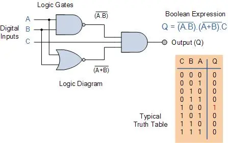
Figure 1: Full Adder Circuit, Truth table, and Boolean expression
Sequential Logic Circuits
Output is dependent on current and past inputs in sequential logic circuits. The information is stored in a digital circuit through sequential logic circuits and memory is stored in these circuits. Latch is the sequential logic circuit's simplest component. Latches could be called flip flops. The loop is regarded as the combination circuit wherein one or several outputs are returned as inputs. Typically utilized are SR (Set–Reset), JK, T (Toggle) and D flip flops. Sequential logic circuits are used in each cycle for memory components. In sequential logic circuits, clock is used. It activates the process of the flip flop.
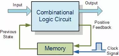
Figure 2 : Block Diagram of Combinational Logic Circuit
|
Sequential Logic Circuits |
Combinational Logic Circuit |
|
There are components of memory in it. |
There are no components of memory in it. |
|
The current output value relies on the inputs value and past value. |
The existing output value relies on the current input value. |
|
It is possible to store the information in digital circuits. |
It is not possible to store information in digital circuits. |
|
They are clock-independent. |
They rely on the clock. |
|
There is a need for feedback circuits. |
There is no need for feedback circuits. |
Alarm system used in measuring, evaluation and identification of faults and changes needed
The support structure is used to handle unusual incidents. This method of assistance is identified as the alarm system. It is the main framework of assistance for the operator. The user is alerted by it about the system's anomaly. The alarm system is able to predict the threat. The alarm system is used to warn, notify and direct the user about the unusual incident. The appropriate response should be indicated at the moment. It must have a pace at which the user can address the issues and that should be easy to comprehend. The alarm system should also be available in all operation situations. It should be carefully designed. To identify the defect, the fault finder tracker is used. If a defect arises in any line it is possible to identify the position of the problem by the alarm. Often recognized as the smoke detector, the alarm system is used to detect smoke.
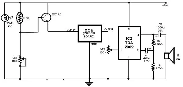
Figure 3 : Smoke Detector Circuit
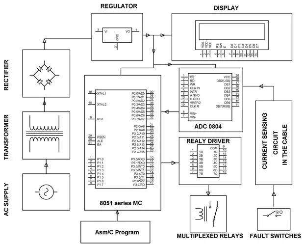
Figure 4: Circuit diagram of underground cable fault distance locator
If an underground wire is discovered to be a defect, the above circuit can identify it. Determining the position of the flaw in order to fix it is very critical. This follows the principle of the law of Ohm. This uses the 8051 microcontroller. The ADC unit calculates the wire length (in KM). A relay driver integrated circuit governs the relays. The wire connections are tested using it. A microcontroller is attached to an LCD unit, which is used to read the data. Different electrical or physical terms are calculated using a certain procedure. This method is called the Data Acquisition (DAQ). The variables that are calculated by DAQ are sound, voltage, pressure, current and temperature.
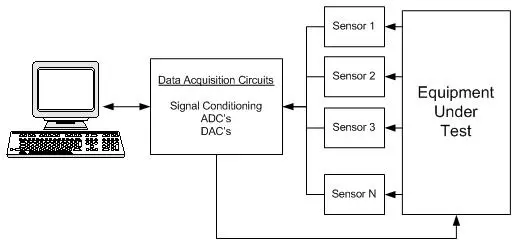
Data Acquisitions Block Diagram
The above block diagram describes the process of data acquisition of equipment under observation. Different sensors are mounted on the appliance. DAQ links these sensors to a computer The circuit upgrade is ordered by DAQ. Upon checking the device, this increases the device's quality and performance. It can also improve the efficiency of the underground wire fault tracker. If the microcontroller is attached to the DAQ circuit and alarm system, the alarm system can quickly find the error and, at the same moment, show the position of the defect on the screen. It will increase the system's performance and reliability.
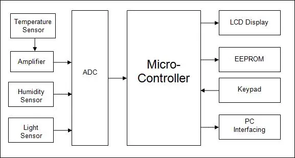
Figure 6: DAQ using 8051 microcontroller
In the previous page, the schematic of DAQ using 8051 microcontroller was shown. The diagram shows all the necessary tools. To improve its efficiency, a system should have all those required equipment. If the microcontroller is attached to the DAQ circuit it will be convenient for the device to retrieve information. Human interface in any program plays an important role. The human being should engage appropriately with the computer to improve the device's efficiency. Only the user interface will make it possible to link the other devices. Therefore, all the necessary devices in a network should be linked to improving application efficiency. Full adder circuit assignments are being prepared by our electrical engineering assignment help experts from top universities which let us to provide you a reliable top assignment help service.
Bibliography
VanCamp, K. (2016). Alarm management by the numbers. Chem. Eng. Essentials CPI Prof., Autom. Control.
Larsson, J. E., Öhman, B., Calzada, A., Nihlwing, C., Jokstad, H., Kristianssen, L. I., ... & Lind, M. (2006, November). A revival of the alarm system: Making the alarm list useful during incidents. In Proceedings of the 5th International Topical Meeting on Nuclear Plant Instrumentation, Controls, and Human Interface Technology, Albuquerque, New Mexico.
Bransby, M. L. (2000). Best practice of Full Adder Circuit in alarm management.
Leva, M. C., Naghdali, F., & Alunni, C. C. (2015). Human factors engineering in system design: a roadmap for improvement. Procedia CIRP, 38, 94-99.
John, M., Joseph, A., & Vasanthi, D. (2017). Design and implementation of low cost Full Adder Circuit in multichannel data acquisition hardware for computer aided measurement. In 2017 Trends in Industrial Measurement and Automation (TIMA) (pp. 1-4). IEEE.
Hypolite, K., Wolf, J., Brun-Kestler, A., & Brun-Kestler, M. (2015). U.S. Patent Application No. 14/583,710.
Piccolo III, J. (2015). U.S. Patent No. 8,988,217. Washington, DC: U.S. Patent and Trademark Office.


